Electrical Analysis
Real-time On-line Product Analysis Database
Tracing the history of a failure mode/mechanism to reduce analysis cycle time, recognize trends and track ongoing analyses
WLCSP & BGA Rework/Re-ball Roolset
Package reconditioning for test capability
Open/Short/Leakage Parametric Testing
Parametric failure replication - ability to connect to all device pins over a wide range of package types
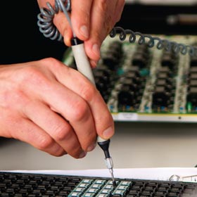
ATE Testers and Evaluation Board Setups
Functional failure replication - analysis requires ability to fully exercise the failure mode while allowing access to device circuitry
Package X-ray, Acoustic Microscopy
Package integrity inspection
Topside Package De-capsulation
Unsurpassed decapsulation capability ranging from 5 pin TSSOPs to 352 BGAs while maintaining device functionality
Backside Package De-capsulation
Access to the die backside surface enabling through silicon analysis techniques
Near IR Optimized Light Emission Analysis (LEM)
Near infrared offers enhanced front side or through silicon capability for this time-saving analysis shortcut
Laser Scanning Microscope (LSM) & InGaAs Emission
Capability of performing die topside and backside LEM, OBIRCH, TIVA diagnostics, as well as advanced fault isolation technics like LVP, LVI and SIL
CAD Software Tools
Circuit and mask layer navigation and cross linking for debug
Focused Ion Beam (FIB)
Probe access point creation and circuit modifications
Functional Micro-probing
Method of tracing a failure by probing through circuitry to pin point the failure - time consuming, but necessary at times
Nanoprobing
Fault isolation on advanced process nodes, including e-beam absorbed/induced current methods
Atomic Force Microscopy (AFM)
Nano scale electrical characterization utilizing conductive and tunneling imaging
Physical Analysis
Dry and Wet Etch Top-down De-processing
Capability to choose the correct deprocessing method for the type of defect isolated by electrical analysis
Dual Beam FIB
Precision cross-sectioning and high resolution imaging
Optical Inspection Microscopes
High resolution water immersion, confocal and laser scanning imaging with integrated digital image capture
Mechanical Cross-sectioning
For rapid inspection and monitoring of Fab processes
SEM/EDS Imaging and X-ray Elemental Analysis
Ultra high resolution imaging for identification of failure mechanisms at the Fab process level
ESD and Latchup
JEDEC Compliant ESD/Latchup Testing
Multi-system in-house testing for rapid design feedback and complete debug capability